Our facilities
World-class facilities for the fabrication of advanced materials and characterization of transport phenomena are hosted in the Nanoionics and Fuel Cell Labs.
Our laboratory is equipped with unique PLD, CVD and ALD thin film deposition systems able to work at wafer-level, which allows the development of nanostructured devices in batch mode. Complementary, such micro-devices can be electrically and electrochemically characterized in several manual and semi-automatic micro-probe stations able to reach exceptional high temperatures (T~700ºC) under controlled atmosphere. Special developments of our group allow in situ/operando characterization of such devices by using multi-wavelength ellipsometry and Raman spectroscopy.
Regarding advanced manufacturing of ceramics, our laboratory holds a hybrid SLA-robocasting 3D printer able to carry out multi-material printing in large volumes. This singular equipment combined with multiple simple printers and robotized deposition systems gives rise to a unique rapid manufacturing platform devoted to functional oxides. The electrochemical characterization of developed ceramic-based energy devices is carried out in a series of automatic test stations with controlled temperature and atmosphere (pO2, humidity, CO2, etc). Two kW-range SOFC and SOEC stations complete the list of outstanding available resources in our lab.
SINGULAR EQUIPMENTS
THIN FILM DEPOSITION AND CERAMIC PROCESSING EQUIPMENT
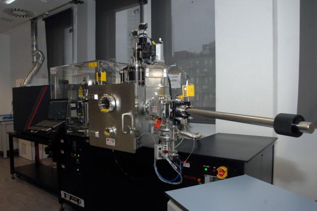
Large-area Pulsed Laser Deposition
PLD 5000 (PVD Products, US) is a large area pulsed laser deposition system. It allows growing ceramic thin films on substrates of up to 10 millimeters of diameter for direct post-processing in the micro electronics industry. A 240 nm excimer laser (Coherent Compex Pro 205F) sends a high energy beam (up to 700 mJ) to the surface of the target material. The system is capable to hold four large area targets. The installed combinatorial option can produce a gradient of compositions along the substrate, which allows exploring the properties of a wide range of species in a single sample.High quality complex oxide thin films deposited in substrates up to 4” in diameter.
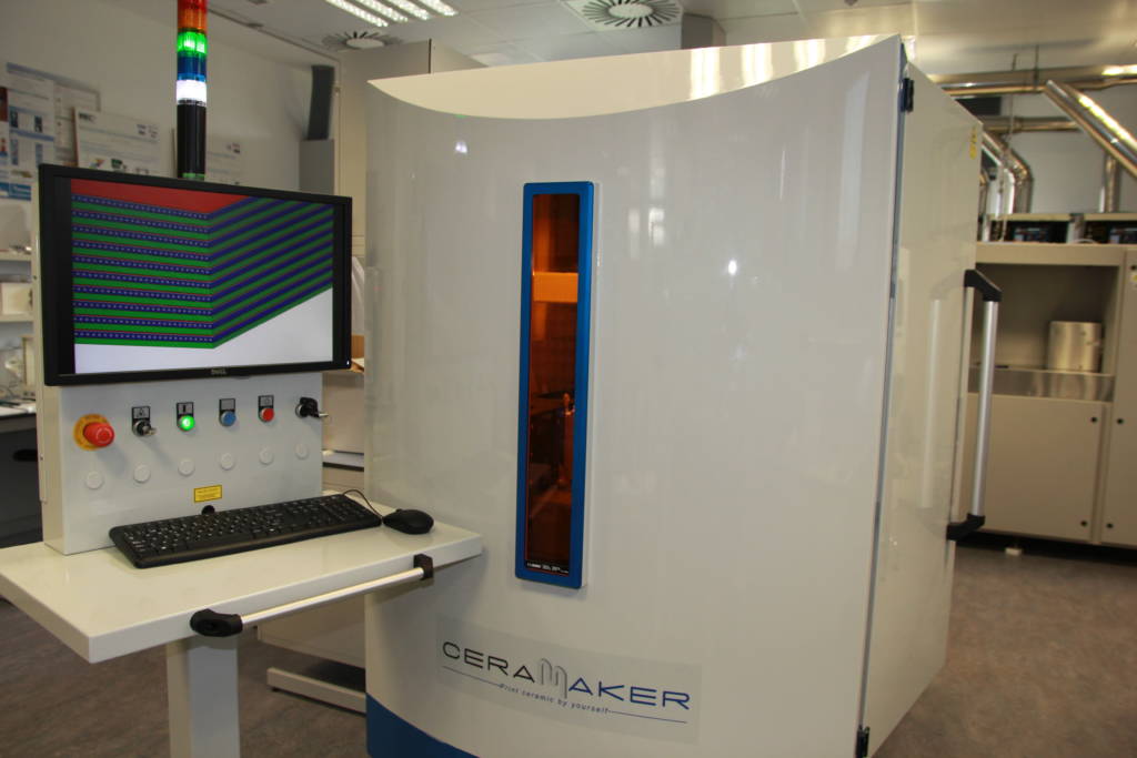
SLA ceramic 3D printer
Ceramaker (3DCeram) is aunique facility based on a hybrid ceramic 3D printer which hybridise SLA and Robocasting techniques. With a printing volume of 300x300x120mm and a resolution of 25 microns, it can print multimaterial ceramic pieces conformed by 4 different materials integrating horizontal or vertical channels.
Chemical Vapor Deposition
EasyTube 3000 (Firstnano) is a chemical vapor deposition system for the synthesis of doped Si-Ge nanowires onto 10 millimeter wafers. This large area capabilities allows post processing in clean room facilities. The deposition can be performed under vacuum and high temperatures up to 1100 °C.
Screen printing
SI-P850 (Sony) is an industrial screen printing equipment capable of depositing onto large area substrates (460mm x 410mm), with a high precision positioning (error below 20 μm). The slurry composition can be selected in order to print ceramic films with the repeatability and process speed (10 seconds process) demanded at the industry.
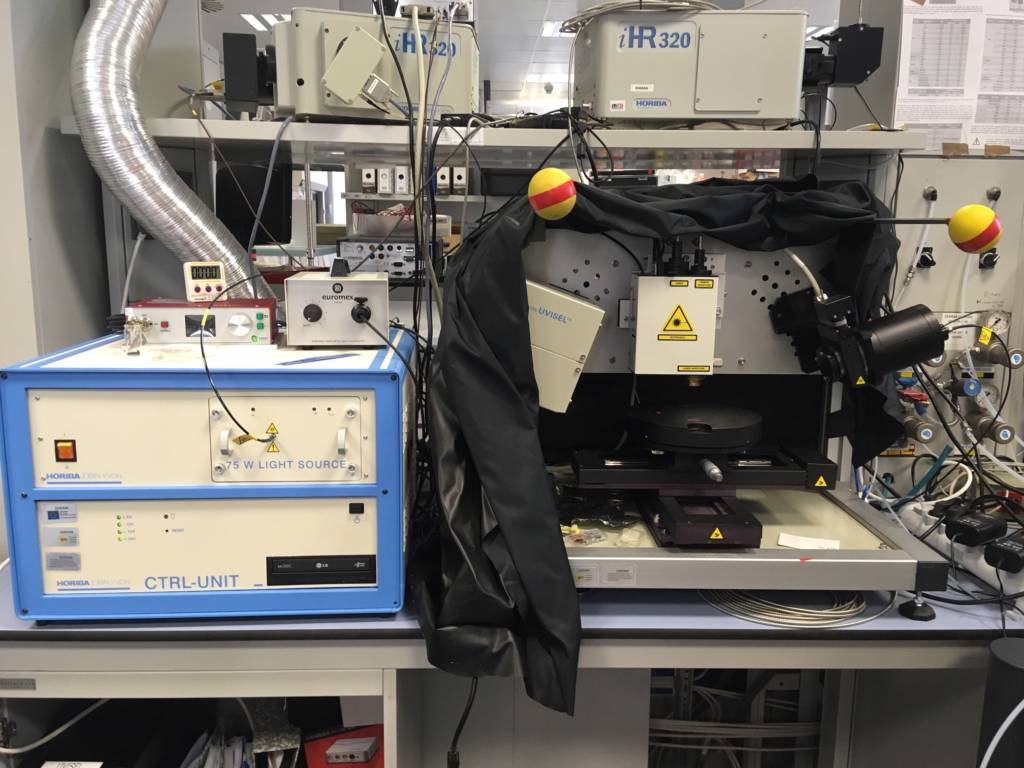
Ellipsometry /Raman
Horiba iHR320 monochromators UVISEL ellipsometry system and Horiba superhead Raman with Horiba syncerity CCD.
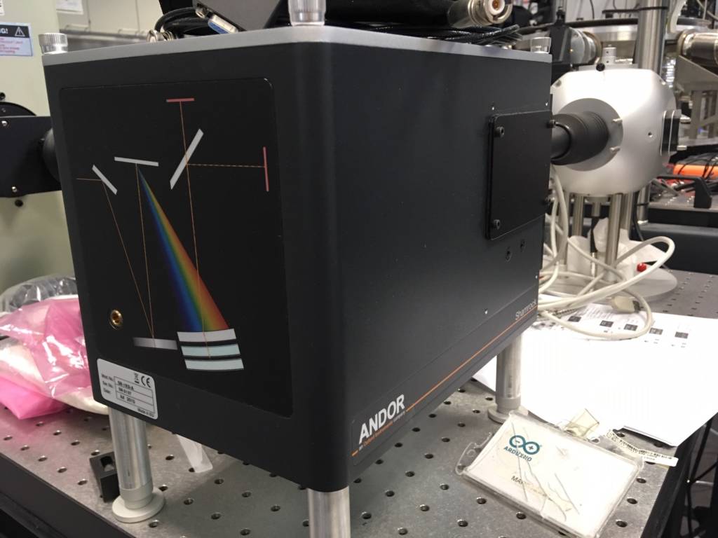
Quantum efficiency
Andor SR193i monochromators + iDus 416 CCD.
Electrochemistry Measurment Stations
FABRICATION AND CHARACTERIZATION
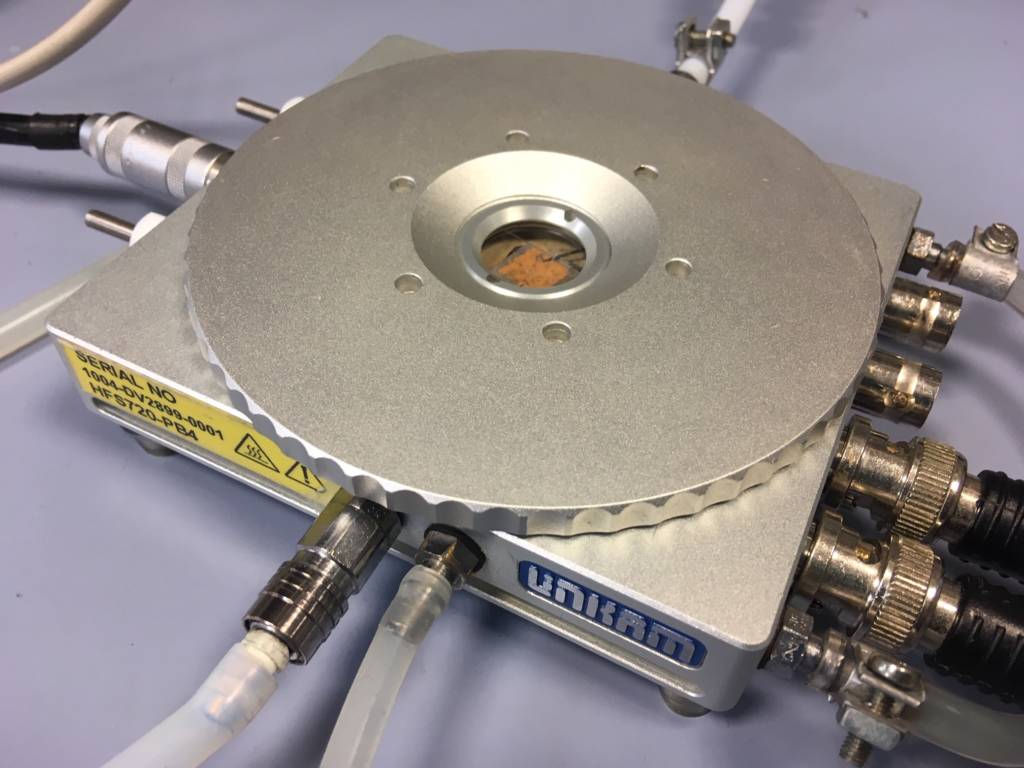
Probostat/Linkam
We have several high temperature measuring chambers adaptable to the particular electrical characterization needed:
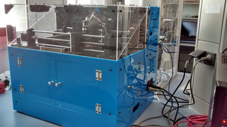
- High temperature microprobe station (Linkam, UK THMS600)
- Semiautomatic high temperature probe station adapted for 4” wafer samples.
- Ceramic-based gas stations coupled with tubular furnaces for high temperature multi-chamber measurements (Probostat NorECs AS)
Inkjet
Print3Dsolutions 4 axis powder bed inkjet printer
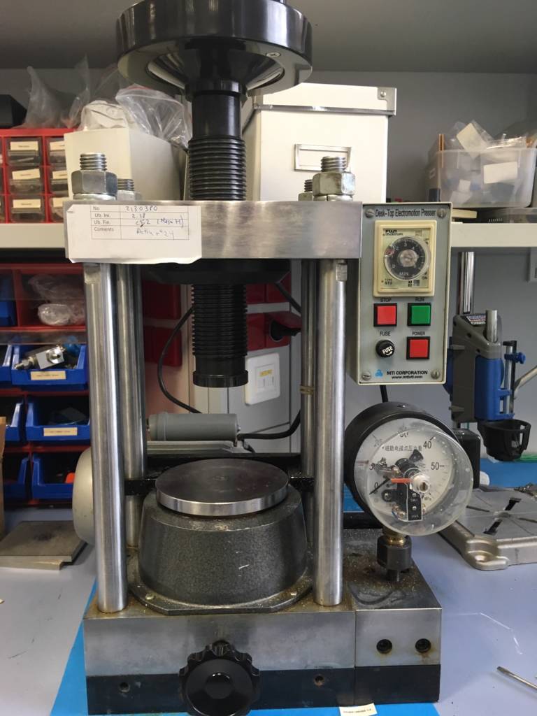
Uniaxial press
MTI, up to 60 MPa
Mtixtl.com
Plastic 3D printers and aerography
print3Dsolutions Prusa i3 3d printer & aerograph.
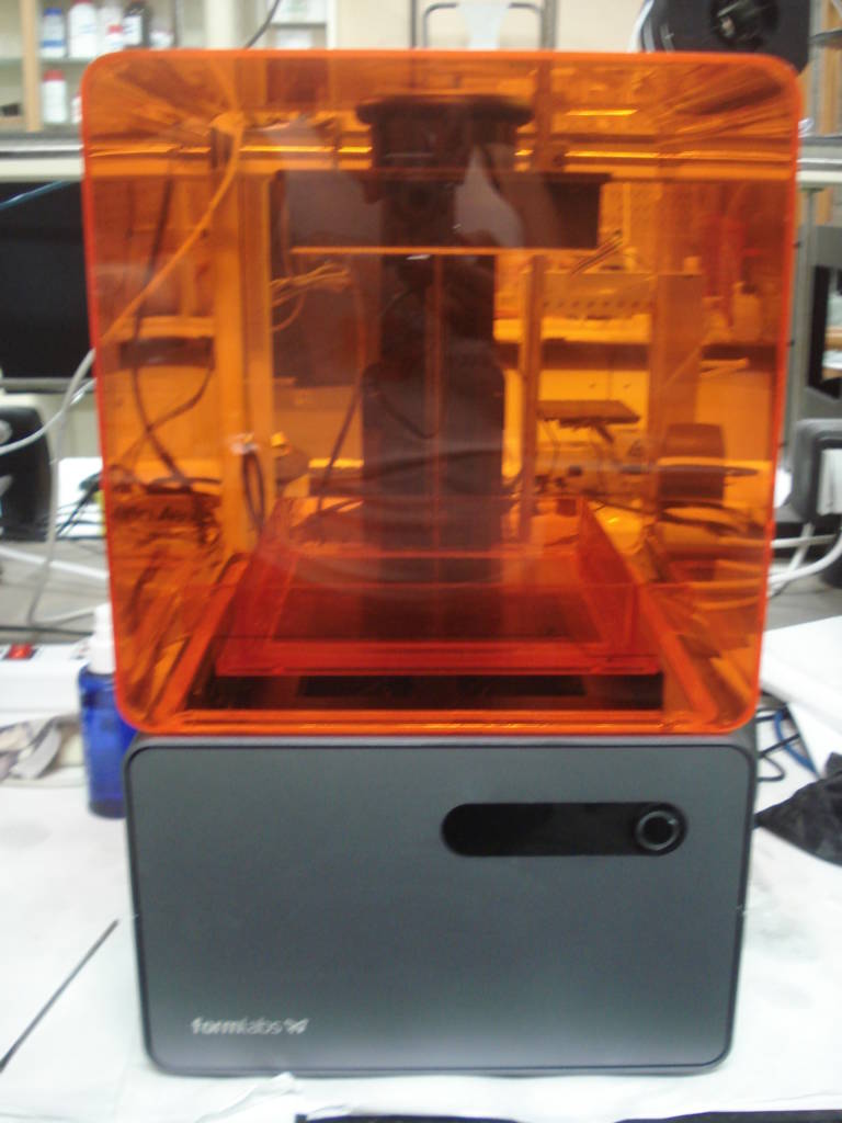
SLA printer Form2 (Formlabs)
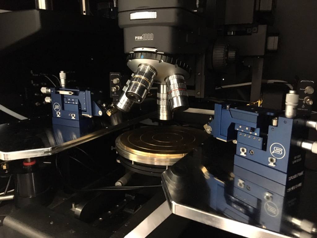
Electroemission
Signatone microscope set-up with Andor SR303i monochromator + iStar DH7 ICCD + Keithley 4200 SCS electric pulsing measurement set-up.
SHARED EQUIPMENT
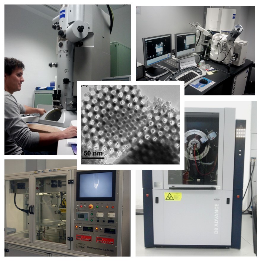
- Scanning Electron Microscopy -Zeiss Auriga / Gemini 30kV schottky FESEM column
- Transmission Electron Microscopy – Zeiss Libra 120 (LaB6)
- Confocal microscopy – Sensofar Plu Neox
- X-Ray Diffraction – Brucker
- AFM – Park Systems XE7
- High temperature furnaces – Hobersal up to 1600 ºC and Lenton up to 1500 ºC
- Cryomagnet IntegrAC with He compressor – Oxford / Sumitomo
- Binocular, straight and inverted optical microscopes – Zeiss
- Contact angle – Dataphysics
OTHERS
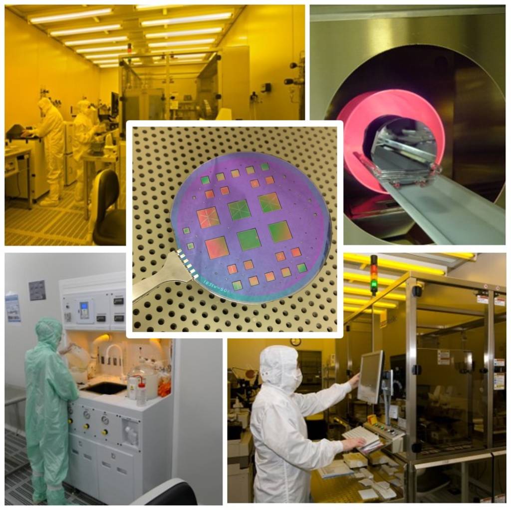
Microfabrication and Clean Room Processing
Our group is one of the few groups with large background and capabilities to integrate thin film ceramic science into microtechnology. Ceramic thin film deposition and characterization is performed at IREC facilities, while the microfabrication is performed at Institute of Microelectronic of Barcelona (IMB-CNM, CSIC), using cutting etch silicon technology. Our group has open access to the clean room thanks to a close collaboration between IREC and CNM.